EMC Compliance PCB Design

EMC-Compliant PCB Design

Minimizing EMI for Reliable Performance

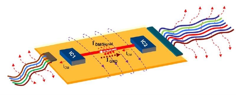
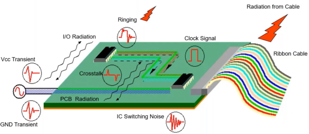
RF EMC compliance in PCB design ensures that electronic devices don’t emit harmful EMI and are immune to external interference, operating within regulated limits. Achieving this requires careful component placement, shielding, grounding, and trace routing to minimize noise and ensure signal integrity in applications like wireless communication and medical devices.

Key Considerations for EMC-Compliant PCB Design

  • Component Placement

    Strategically positioning components to reduce noise and interference.

  • Shielding & Filtering

    Using shields and EMI filters to control electromagnetic radiation and protect sensitive signals.

  • Trace Routing

    Optimizing high-frequency signal paths to reduce crosstalk and reflections.

  • Power Integrity

    Ensuring stable power distribution with decoupling capacitors and low-impedance power planes.

contact now

Get a Quote.

If you have any Query Feel free to Reach Us